
About this manual
This manual describes the design basis, hardware features and interfaces of the ePot V4 LDR attenuator & preamp controller, generally referred to as the V4.
This manual is being frequently edited and updated and is subject to change without notice.
The control and operation of the V4 is covered in a separate manual which can be found here.
What is the ePot.V4
The Pot.V4 is a digitally driven analog circuit board that when equipped with an appropriate power supply and our proprietary OLED display can function as a unity gain passive preamp and overall preamp controller. When equipped with our optional solid state buffer board, the V4 can also function as an active preamp with adjustable gain.
The V4 builds on 15 years of LDR preamp controller evolution and is intended for use by DIY audio enthusiasts and audio OEMs. Tortuga Audio has used similar hardware in building its own line of finished preamp products and may do so again in the future.
Like all Tortuga Audio preamp controllers, the V4 employs light dependent resistors (LDRs) as voltage dividers for volume control. The V4 has no moving parts as do conventional volume controllers that use mechanical potentiometers or mechanical switched attenuators.
The V4 is an evolution of our earlier V3 series.
V4 vs. V3 design changes
The ePot.V4 combines everything we learned to date about previous models, retains all the positives, with the result being our best LDR attenuator/controller ever. Here are the key design changes.
| V3 | V4 | Commentary | |
|---|---|---|---|
| Processor | – STM32F2 microcontroller – M3 ARM Cortex – Single core – 12 bit internal ADC for measurement | – STM32G4 microcontroller – M4 ARM Cortex chip – Dual core – Math processor – 16 bit internal ADC | – The newer V4 chip has several advanced features including a faster clock, a built-in math processor, and ability to achieve effective 16 bit pulse-width-modulated output and 16 bit analog-to-digital measurement with oversampling. – Allows for the elimination of a costly external DAC chip without sacrificing control accuracy. – Improved calibration measurement accuracy – Improved adaptive calibration algorithm |
| Signal switching | – low distortion analog switches running on split +/- 5 volt power | – conventional electro-mechanical miniature relays | – Although generally successful, the analog IC switches used in the V3 series were found to be incompatible with certain audio source devices where incoming audio signals would disrupt the operation of the controller by interacting with the power supply through the analog ICs. Therefore, we chose to use conventional electromechanical relays for the V4 for improved stability and reliability. |
| Inputs | – Selects between 6 stereo input devices | – Selects between 4 stereo input devices | – The physically larger relays used by the V4 meant we could only fit 4 inputs compared to 6 inputs for the V3 while keeping the boards the same size for upgrading compatibility. |
| LDR current control | – External 16 bit DAC chip outputs | – Native 16 bit pulse width modulated outputs | – The V4 employs a simpler approach with reduced part count at a lower cost. |
| Power supply | – Requires external 12 volt 0.5 amp DC power source – Uses switching DC-DC regulator to generate 5 volts on board – Uses linear regulator to generate 3.3 volts on board | – Requires external 5 volt 0.5 amp DC power source – No switching regulators – No split voltage – Generates 3.3 volts from internal linear regulator | – The V4 eliminates the complexity of a split voltage power supply for the main board – V4 performance benefits from clean external power |
| Muting relay | – no relay – partial muting achieved via LDRs only | – dedicated muting relay shunts output to ground providing full muting | First LDR based controller to provide full muting |
| Firmware updating | – Requires use of external USB to UART converter board or cable | – Firmware updating via direct USB connection | – Requires use of a free vendor supplied STM32CubeProgrammer application compatible with PC, Mac and Linux machines. |
The V4 board
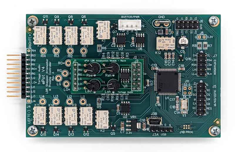
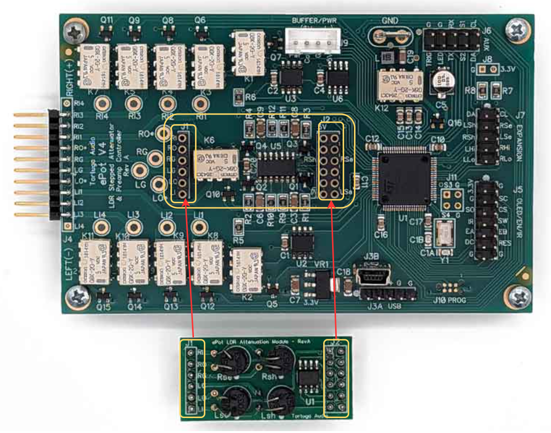
The initial Rev A version of the ePot.V4 board was released in December, 2024 and is shown below with annotation. Individual parts on the V4 board are identified by their reference designator (J2, U4, C18) and most are discussed in the sections below.

The V4 board is a 2-layer printed circuit board that is 2.7 inches wide and 4.25 inches long. The V4 is the same width as the V3 but is 0.15 inches shorter. The overall height including the plug-in LDR module is slightly greater than 1 inch but we recommend allocating 1.5 inches of vertical space above the board; 2 inches if you opt for the solid state buffer board addition. There are no parts mounted on the underside of the board but a minimum clearance of 0.125 inch is recommended underneath the board to avoid making contact with any through-hole soldered parts and to allow for adequate air circulation.
In addition the the primary V4 board shown below, there’s a similar V4 expansion board (not shown) that is used in combination with the primary V4 board for balanced audio applications.
Volume control basics
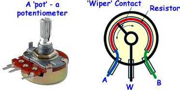
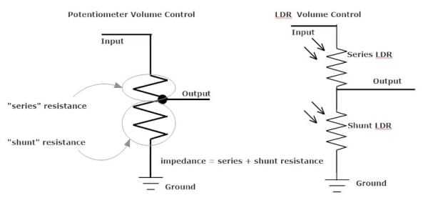
The V4 emulates the behavior of a conventional volume control potentiometer, or “pot”, which are essentially voltage dividers. In lieu of using a potentiometer, each V4 utilizes 2 pairs of discrete light dependent resistors (LDRs). LDRs can be configured to behave similarly to a pot.
Whereas a pot is a mechanical device and must be rotated by hand (or electro-mechanical drive) to affect changes in volume, LDRs have no moving parts and must be controlled electronically.
The governing equations for this method of volume control are as follows:
- RSeries = the resistance level in ohms of the series LDR (resistance above the output wiper)
- RShunt = the resistance level in ohms of the shunt LDR (resistance below the output wiper)
- Voltage Ratio (VR) = the ratio of RShunt / (RShunt + RSeries)
- Vout = Vin x VR
- Impedance = sum of RShunt + RSeries
- dB attenuation = 20 x log10 (VR) ….or…. 20 x log10 (RShunt / (RShunt + RSeries)
More information on LDRs and how LDR volume control works can be found here.
Introduction to Light Dependent Resistors | LDRs
Light dependent resistors (LDRs) are at the core of Tortuga Audio’s preamp controller & stepped attenuators including the V4.
LDRs are a type of resistor where their level of resistance varies in proportion to the control current applied. LDRs combine two distinct analog electronic devices – a light emitting diode (LED) and a photoresistor, An LDR integrates an LED and photoresistor into a sealed package approximately the size of an M&M candy. LEDs do what their name says – they emit light. Photoresistors are made with a photoreactive semiconductor material that changes resistance based on the intensity of light impinging on the photoreactive material. The intensity of the light from the LED is controlled by regulating the current running through the LED. As the current increases, the light intensity increases and the LDR resistance decreases.
When employed in an audio preamp, LDRs can literally control volume using light! However, due to the complex and variable relationship between current, light intensity and the resulting resistance, the application of LDRs for volume control is technically challenging. LDRs also exhibit higher distortion than conventional volume control devices like potentiometers or discrete resistors which many designers deem to be a disqualifying characteristic.
Nevertheless, we use LDRs for volume control for one very simple reason – music sounds better to our ears with LDR volume control. If music didn’t sound better with LDRs, then what would be the point?
Precision LDR current controller
Since the resistance level of an LDR is proportional to the control current being applied, we need a reliable and repeatable means of controlling that current. We achieve this by using a precision LDR current controller similar to that shown in the diagram below. The LDR current controller employs a precision op amp together with a transistor and current sense resistor to create create a precision high speed closed loop controller that accurately achieves a target current level in response to a command voltage from a microcontroller.
Use of a precision op amp is key to this design. Precision op amps are optimized for applications where high accuracy, low noise, thermal stability, and minimal offset are essential to achieve precise signal processing.
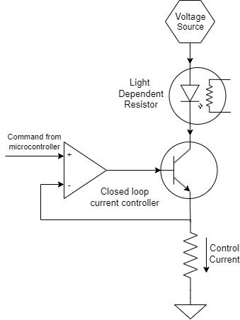
The governing equation for the current controller is relatively straightforward as shown below.
Control current (Ic) = Voltage command (Vc) / Resistance (R).
The control current (Ic) is the current running through the LDR. The resistance (R) is the fixed resistance of the sense resistor. And the target setpoint to the op amp is a voltage command (Vc) that is generated by the V4’s microcontroller.
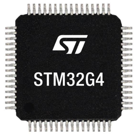
The microcontroller (U1) & LDR calibration
Overall control of the V4 is handled by a proven 80 pin STM32G4 embedded 32 bit ARM Cortex microcontroller. The V4 application code (firmware) runs on this microcontroller chip. The firmware can be updated by the user via the USB interface provided on the V4 board together with a free STM32CubeProgrammer application which can run on the users PC, Mac or Linux machine.
The microcontroller sends a command voltage to each LDR current controller. It does so using a well established technique knows as “pulse width modulation” or PWM. The microcontroller PWM peripheral employs 16 bit PWM timers which divides 3.3 volts into 65,535 discrete steps of 50.35 microvolts per step. This gives the V4 very fine control over volume level allowing for volume control increments of ~0.6 dB which is very smooth indeed, is far superior to any stepped attenuators using discrete resistor pairs, and is indistinguishable (to the human ear) from continuous analog control.
The relationship between control current and resistance is unique to each LDR. Moreover, this relationship is non-linear which is another way of saying that the relationship also varies as the resistance varies. This type of nonlinear behavior in electronic components makes using LDRs for audio control especially challenging.
Tortuga Audio solves this challenge by employing a proprietary software driven calibration process that literally measures the nonlinear behavior of each LDR. The measured current vs. resistance data for each of the 100 volume steps for each of the 4 LDRs are stored in an EEPROM memory chip. This process normalizes the performance of any set of 4 LDRs regardless of their inherent differences.
During normal operation, the V4 microcontroller uses the stored calibration data to set the resistance level of each LDR to achieve the volume level associated with each volume step.
More information on the calibration process can be found here.
Stepped attenuation | 100 volume steps
The V4 breaks volume control into 100 discrete steps of ~0.6 decibels per step over a 60 decibel control range for each of the 4 LDRs used for 2-channel stereo volume control. This requires 400 separate calibration operations per calibration cycle. At this level of granularity, volume change between each step is smooth and continuous with no audible artifacts. There are no noisy mechanical switches or other moving parts involved as compared to conventional mechanical volume control devices like rotary potentiometers or switched stepped attenuators.
Each step change in volume can be made using either a handheld remote control or by using a rotary encoder (control knob) attached to the V4.
LDR module | J1 & J2
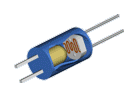
Tortuga Audio uses a proprietary LDR module which incorporates 2 pairs LDRs into a replaceable plug-in module as shown below. The LDR module header pins J1 and J2 plug directly into the matching sockets J1 and j2 on the V4 board.
There are 2 versions of the ePot LDR module – Rev A and B. Rev A (shown below) has the U1 memory chip while Rev B does not. The Rev A module is also referred to as the V3 module while the Rev B is the V4 module. The Rev A/V3 module will work on a V4 board but a Rev B/V4 module will not work with a V3 board.
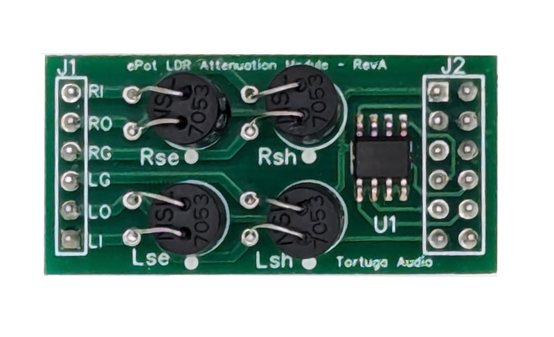
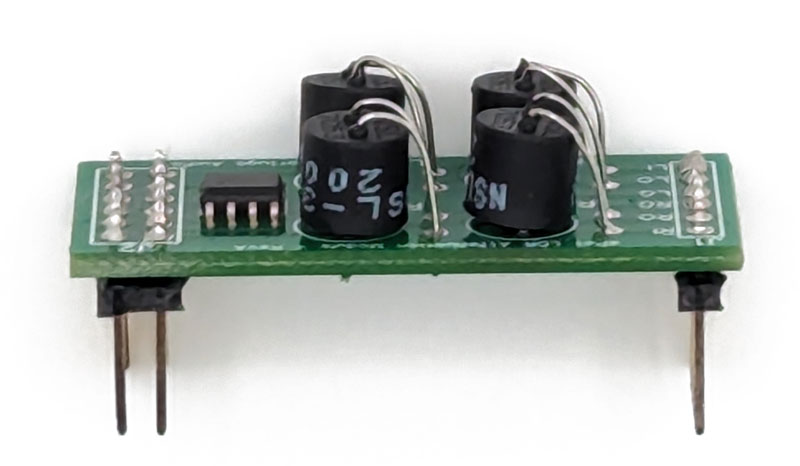
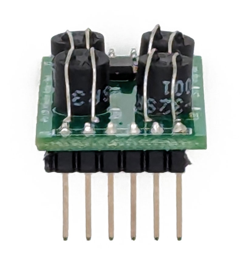
Each ePot LDR module has 4 LDRs configured as two pairs. The topmost LDR pairs (RSeries and RShunt) are the right channel LDRs and the two bottom LDR pairs (LSeries and LShunt) are the left channel LDRs. If an LDR ever fails or goes out of specification, it’s a straightforward matter to replace the plug-in LDR module.
J1 header pinout | all ePot LDR modules
The 6-pin J1 header carries the audio input and output signals plus signal ground for both the left and right channels. Each of these two channels are fully independent of the other including audio signal ground. The J1 pinouts are as follows:
- RI – right input
- RO – right output
- G – right ground
- LG – left ground
- LO – left output
- LI – left input
J2 header pinout
The 12-pin dual row J2 header provides the power, control, and communications. The Rev B module has no communications signals because the Rev B module has no memory chip. The pinouts of each ePot LDR module are listed below.
Rev A – V3 module
- #1 – +5V power
- #2 – -5V power
- #3 – ground
- #4 – N/C
- #5 – right shunt LDR current
- #6 – right serial LDR current
- #7 – SPI chip select
- #8 – SPI MISO (serial data out)
- #9 – SPI clock
- #10 – SPI MOSI (serial data in)
- #11 – left shunt LDR current
- #12 – left series LDR current
Rev B – V4 module
- #1 – +5V power
- #2 – no connection
- #3 – ground
- #4 – N/C
- #5 – right shunt LDR current
- #6 – right serial LDR current
- #7 – N/C
- #8 – N/C
- #9 – N/C
- #10 – N/C
- #11 – left shunt LDR current
- #12 – left series LDR current
To insert the LDR module into the V4 sockets, first align the pins on the 12-pin J2 header into the J2 socket with the LDR module held tilted up lengthwise at a slight angle (J1 end up, J2 end down), then lower the J1 header pins into the J1 socket making sure the pins align. Then gently press the module into both sockets. DO NOT FORCE IT! If the pins are not perfectly aligned into their socket holes, do not expect the module to go in. Re-align the pins on both ends first before attempting to press the module into the sockets. If the module won’t align and go in, visually inspect the pins on the LDR module to see if any pins are slightly bent or out of alignment. The pins can usually be easily manually manipulated back into alignment.
Single-ended vs. balanced audio
By itself, the V4 board only handles single-ended audio. A secondary V4 expansion board is required for balanced audio. Information on the balanced audio expansion board will be added at a later date.
In balanced audio applications the primary V4 board serves as the right channel controller for both the positive and negative right channel phases. Conversely, the secondary expansion board handles the two phases for the left balanced channel. Within each board, there’s a Right(+ phase) channel and a Left(- phase) channel. Thus for balanced audio the V4 actually provides 4 separately attenuated audio signals, 2 for the right stereo channel and 2 for the left.
Power supply | J9 header
The V4 requires an external 5 volt DC power supply with a nominal capacity of 0.5 amps although actual current demand is typically no more than 0.3 amps. The V4 also uses 3.3 volts that it generates internally using a low noise on board linear voltage regulator powered by the external 5 volt source.
The external 5 volt DC enters the V4 board through the 4-pin J9 header on the V4 board. J9 is a 4-pin 0.1 inch pitch shrouded JST male header with the following pinout:
- J9.5V – 5 volt DC regulated
- J9.G – ground
- J9.Cal – calibration enable signal from the V4 to optional buffer board
- J9.Pwr – power enable signal from the V4 to optional buffer board
“JST” type connectors are either made by the Japan Solderless Terminal company, or by other manufacturers using the same connector design.
Only the J9.G (ground) and J9.5V (+power) pins are needed for powering the V4 board. The J9.Cal and J9.Pwr pins are only used when the optional solid state buffer board is present. When a solid state buffer board is installed on top of the V4, power to the V4 is provided by the buffer board through the J9 header.
Audio signal inputs & outputs | J4
The V4 Max can accommodate stereo audio inputs from up to 4 different audio sources and allows the user to switch between these sources at will. There is only a single stereo output. All audio signal switching is done with miniature electromechanical relays. When the V4 is muted, the audio outputs (RO & LO) are switched to audio signal grounds (RG & LG), effectively killing the output. During calibration, both the inputs and the output are disconnected by relays.
Audio input, output and signal grounds to the Max board can be terminated via either the 12-pin J4 header or a separate collection of larger solder pads. These connections are identified as follows:
- J4.RI4 | right input #4 | relay K7
- J4.RI3 | right input #3 | relay K5
- J4.RI2 | right input #2 | relay K4
- J4.RI1 | right input #1 | relay K3
- J4.RO | right output | muting relay K6
- J4.RG | right signal ground
- J4.LG | left signal ground
- J4.LO | left output | muting relay K6
- J4.LI1| left input #1 | relay K8
- J4.LI2 left input #2 | relay K8
- J4.LI3| left input #3 | relay K8
- J4.LI4| left input #4 | relay K8
The left and right signal grounds (LG & RG) are fully independent and DO NOT connect within the V4 board to the power supply ground.
OLED display header | J5
J5 is a 14-pin dual row (2 x 7) header that carries the power and control signals for the OLED display module, the IR receiver module, and the rotary encoder. The IR receiver and the encoder are both part of the OLED display module.
The OLED display module is an essential part of the the V4 board design providing an interactive menu driven visual interface for control and operation of the V4. More information on the OLED display module can be found here.
The J5 header pins are labeled as follows in the clockwise direction:
- J5.3V3 – 3.3 V DC power
- J5.G – ground
- J5.SC – SPI serial data clock
- J5.CS – SPI OLED chip select
- J5.SW – encoder switch
- J5.EB – encoder leg B
- J5.RES – OLED reset
- J5.G – ground
- J5.G – ground
- J5.DC – OLED data/command select
- J5.EA – encoder leg A
- J5.IR – IR receiver signal
- J5.SO – SPI serial data
- J5.__ – no connection
Expansion board header – balanced audio | J7
For balanced audio applications, the V4 Max requires connection to a separate expansion board that connects to the primary V4 board via a 14-pin ribbon cable connected between the J7 headers on each board. The primary V4 board controls the expansion board directly through the J7 header as the expansion board has no microcontroller of its own.
[image of expansion board goes here]
In balanced audio applications the primary V4 board handles the right channel (both the positive and negative phases) while the expansion board handles the two phases of the left channel. Thus for balanced audio the V4 provides 4 separately attenuated audio signals; 2 for the right stereo channel and 2 for the left stereo channel.
The J6 pins are labeled clockwise from top-left as follows:
- J7.DA -I2C serial data
- J7.CL – I2C serial clock
- J7.5V – 5 volt power
- J7.3.3V – 3.3 volt power
- J7.RSe – right expansion serial LDR command voltage
- J7.LSe – left expansion serial LDR command voltage
- J7.RHi – right expansion channel high side measured voltage
- J7.RLo – right expansion channel low side measured voltage
- J7.LLo – left expansion channel low side measured voltage
- J6.LHi – left expansion channel high side measured voltage
- J6.RSh – right expansion shunt LDR command voltage
- J7.LSh – left expansion shunt LDR command voltage
- J7.G – ground
- J7.VRef – calibration ADC reference voltage
Auxiliary status & communication header | J6
The J6 auxiliary header is not necessary for the operation of the V4 but provides additional status and communication options for the user’s designs.
J6 is an 10-pin dual row (2×5) male pin header that provides several logic level status output signals, a 5 volt trigger out signal, plus both UART and I2C serial communications ports for communication with 3rd party external devices.
J6 status outputs are logic level (3.3V) signals only and should NOT be relied on to source or sink more than a few milliamps of current. The J6.LED signal can directly drive a typical LED equipped with an appropriate current limiting resistor. The J6.TRIG signal is a robust 5 volt but requires an external 5 to 12 volt boost to achieve a true 12 volt trigger output.
The J6 pinouts are labeled clockwise from upper left as follows:
- J6.G – ground
- J6.G – ground
- J6.RX – UART serial communication receive
- J6.S1 – unassigned spare output #1
- J6.CL – I2C serial communication clock
- J6.DA – I2C serial communication data
- J6.S2 – unassigned spare output #2
- J6.TX – UART serial communication transmit
- J6.LED – unit on/off status signal for panel LED
- J6.Trig – 5 volt trigger output (relay switched)
Solid state buffer board (optional)
The V4 Max can accommodate an optional solid state buffer board (sold separately) that mounts directly on to the V4 board using the same sockets as the LDR Module. The LDR Module is then plugged into the solid state buffer board.
The buffer board turns the V4 Max into an active solid state preamp with adjustable gain.
The manual for the solid state buffer board can be found in a separate section [** TBD **].
Firmware updating
The firmware updating procedure for both the Max and Mini can be found in a separate section [ ** TBD **].
Ambient requirements
The V4 is designed to operate within nominal room temperature conditions that are typical for home stereo equipment. LDRs are known to be temperature sensitive. Therefore large departures from nominal home room temperature conditions may cause the LDR attenuation module to operate poorly. Operating an LDR attenuator module inside of equipment that gets very warm may still work but you may have to run calibration after board has warmed up and stabilized. We have not found this to be a problem within our own preamp products but the caution is valid.
