
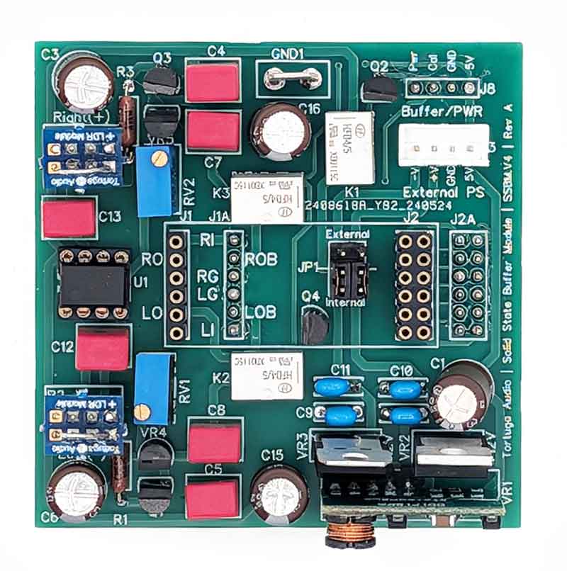
What is the SSBM.V4?
The SSBM.V4 is a solid state audio buffer module that plugs into the ePotPi.V4 Stepped Attenuator & Preamp Controller board in order to convert the V4 from a passive to an active preamp/attenuator.
The purpose of an audio buffer is to act as a current or energy amplifier. An energy amplifier doesn’t make the music louder – that’s the job of a regular amplifier that makes music louder by increasing its voltage level. An energy amplifier (i.e. buffer) makes sure the energy in the music is delivered with optimal dynamics at any volume level.

Another key characteristic of buffers if they have high input impedance together with a low output impedance. Any source connected to a high impedance buffer will not have to work hard to deliver its audio signal thereby preserving audio quality. Conversely, a low output impedance will make it easier for the output signal from a buffer to deliver its audio energy (voltage & current) across the full frequency spectrum – typically to a power amplifier.
The net benefit of a buffer is a more robust and coherent audio signal with more authority, especially during high energy transient passages associated with striking drum heads, plucked strings, or other energetic signals with high initial attack. Simply put, music usually sounds better when properly buffered.
Key features
The features of the SSBM are summarized in the following list.
- Plug-in board integrates fully with the V4 Max via the three sets of sockets
- Power on/off and LDR calibration mode controlled directly by the V4 Max
- Once installed, the LDR module plugs into the SSBM board’s own sockets
- Direct audio input and output – no coupling capacitors
- DC offset of outputs are manually adjustable to near zero and remain stable
- Dual channel socketed 8-pin DIP op-amp input stage | can easily accommodate alternate plug-in op-amps
- Adjustable gain from unity to +12 dB via plug-in resistor gain modules
- High performance constant current JFET output stage
- Powered by external 5 volts DC that also powers the V4 Max board
- Two stage internal switching DC-DC converter provides split voltages followed by second stage linear regulators for clean +/- 12 volts
Hardware versions
Two versions of the SSBM.V4 have been released. Version A of the Solid State Buffer Module was released in January 2025. Version B was released a few months later in May.
The key changes to Rev B over Rev A include:
- Improved split voltage dc-dc regulator
- Isolated ground for lower noise
- space for optional positive & negative super regulators
- eliminated optional external split voltage power
- use of low ESR ceramic vs. polarized electrolytic capacitors
Buffer board stack-up
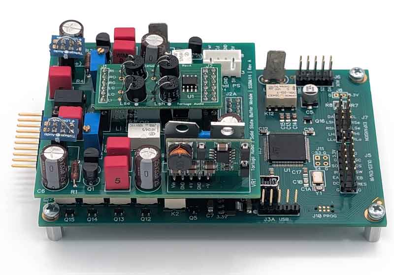
When the solid state buffer module is used, it creates a 3-layer hardware stack as approximated by the illustration below. The buffer module plugs into the V4 Max board and the LDR Module plugs into the buffer module.
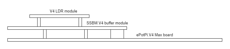
The 3 male headers J1A, J2A, & J8 on the underside of the SSBM board are for mounting the SSBM directly to the V4 board via sockets V4.J1, V4.J2 and V4.J8. Please note that the plug-in LDR Module must first be removed from the V4 board before inserting the SSBM board to the V4. Once the SSBM is mounted on the V4 board, insert the plug-in LDR Module into SSBM.J1 and SSBM.J2 same as you would with the V4 board.
Buffer design basics
Adding the optional buffer module to a V4 board, transforms the V4 preamp from a passive into an active preamp. It becomes an active preamp by virtue of introducing a power supply directly into the audio signal pathway.
When the SSBM.V4 Solid State Buffer Module is present, the output of the otherwise passive V4 Preamp Attenuator/Controller becomes the input to the 2-stage active buffer as shown in the diagram below.
The first stage of the buffer is the input stage consisting of an op amp with high input impedance and commensurately low output impedance. The op amp is powered by a +/- 12 volt split supply generated internally from a 5 volt external source. By default, the op amp is set to unity gain (no amplification) with the option to increase gain up to +12 dB by changing plug-in gain modules. Most systems do not require any actual gain from a preamplifier but it’s there if you need it. The output of the op amp fist stage becomes the input to the second stage.

The second stage is the current drive of the buffer. The current drive doesn’t amplify the loudness of the audio signal. Instead, the current drive ensures that there’s sufficient power to deliver the audio signal with optimal dynamic fidelity. The heart of the current drive is a high performance LSK170 JFET type transistor running on the same split voltage supply as the op amp. The output of the second stage becomes the audio signal output.
The SSBM.V4 has no input or output coupling capacitors to block any DC offset is the incoming audio signal. Avoiding blocking capacitors ensures the best possible sound quality, however, DC offsets must also be avoided. To ensure that only the AC component of the audio signal is passed through, the JFET idle current is manually trimmed to ensure near zero DC offset at the audio output. Once trimmed, the DC offset remains fairly stable over time but may occasionally warrant measurement and manual trimming by the end user to ensure optimal performance. This is achieved by tweaking the resistance level of trim pots RV1 and RV2.
During LDR calibration, the buffer board is temporally isolated from its V4 mother board via relays K1, K2 and K3. This is fully automatic and handled by the V4 Max board.
Power supply | 5 volts DC
The V4 buffer board is powered by any external regulated 5 volt DC source rated at 1 amp or higher current. 5 volt power connects directly to the J3 pin header on the buffer board. The J3 power header is not keyed so please be mindful to get the polarity correct to avoid damaging the hardware. The buffer board transmits this same 5 volt DC power to the primary V4 board that it’s plugged into.
The buffer board uses the 5 volt power to derive the +/- 12 volt split voltage needed to power the buffer circuit described above. The split voltage is produced by a special type of switching DC-DC converter that produces +/- 15 volts. These higher voltages are in turn processed through separate +12 volt and -12 volt linear voltage regulators. These default linear regulators can be optionally upgraded with super regulators such as those produced by Sparkos Labs.
Operations
The SSBM.V4 is controlled by the ePot.V4 board into which it’s plugged using 2 discrete control signals that control power on/off to the buffer circuit, and disengage the buffer circuit during LDR calibration.
Physical dimensions
The SSBM board is 2.7 inches per side, the same width as the V4 Max. The overall height of the SSBM when plugged into a V4 Max including the plug-in LDR module is __________ but we recommend allocating ________ inches of total vertical space for the combined V4/SSBM assembly.
Ambient requirements
See V4 Max for requirements.
