
What is the SSPB.V2?
The SSPB.V2 is a 2-stage solid state preamp buffer kit that employs a high quality audio op amp input (voltage gain) stage followed by a JFET output (current gain) stage. The input stage op amp can operate at unity gain or can optionally provide a modest amount of gain (voltage amplification). The JFET output stage provides current amplification (power boost) which gives the audio signal more authority and dynamic punch.
The SSPB buffer does not have its own volume control. It can be placed before or after any preamp with the latter being the most common. Since it doesn’t have its own volume control, a volume control will typically be located immediately upstream of the buffer. The volume control can be a simple volume potentiometer (pot-in-box), a passive preamp type volume control, or any active preamp. It may also be placed downstream of a DAC that has its own internal analog or digital volume control.
When combined with an upstream volume control, the SSPB becomes a simple yet highly effective active solid state preamp/buffer. The buffer accommodates a single-ended stereo signal – 2 channels. Anyone wishing to build a buffer for balanced audio will require 2 SSPB.V2 boards (4 channels).
What’s included?
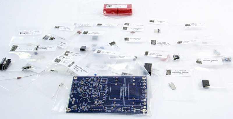
The kit is a single printed circuit board (PCB) plus a collection of parts that must be soldered into place on the PCB. Nothing comes pre-assembled. Every part must be mounted and soldered into place. Some parts are socketed in which case their socket must first be soldered into place before inserting the part into its socket.
The kit comes as a “bag of bags”. Each part or collection of parts comes in its own clear plastic bag with a printed label. It’s highly recommended that you keep everything in its labeled bag until you’re ready to install that part. Each bag will have a part ID as part of its label. That part ID corresponds to the part number printed on the PCB as shown below.
Some parts are optional in which case the detailed assembly instructions below will indicate this and explain the option.
To become fully operational the buffer kit must be provided with a source of 12 V DC power. This power source is not included with the basic kit but can be purchased separately. The kit draws very little current so even a small 0.5A 12V power source will be adequate.
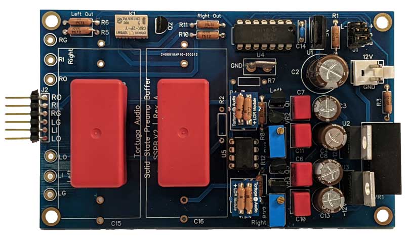
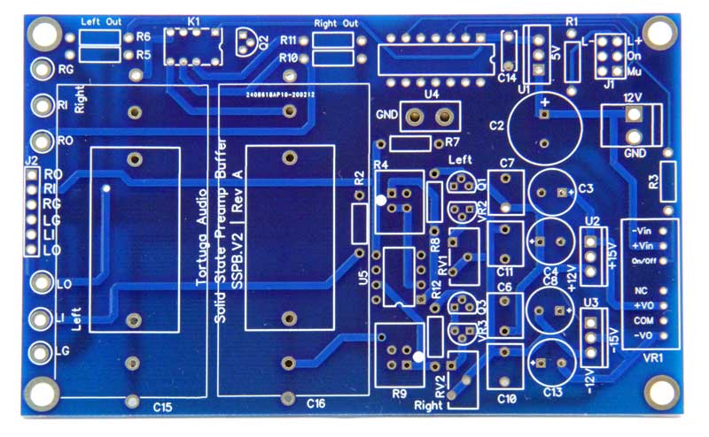
Printed circuit board
The PCB is 4.4 inches wide by 2.7 inches tall. When we refer to locations and parts on the PCB we are referencing the PCB diagram shown above. This diagram is an enlarged version of the actual circuit board with each part identified by a part designator ID such as C2, R11 etc.
The detailed assembly instructions found below make specific reference to each of these parts.
Operation
Overview
If you simply wish to have the buffer turn on and operate any time power is applied to the board, make sure you place jumpers across both the J1.On pins and the J1.Mu pins.
If you wish to control the on/off status of the board and/or mute/unmute the board by some other device you can connect remote signals to pins J1.On and J1.Mu.
Power up
When 12-18 V DC power is applied to the board, the VR1 power regulator will turn on provided that there’s a jumper across the J1.On pins or the J1.On pin is being pulled low to ground. Removal of the jumper across J1.On pins will immediately mute and turn off the board.
Muting
When the board is turned on via jumper across J1.On or J1.On pin being pulled low to ground, a 3 second unmuting timer will start. After 3 seconds the board will unmute provided that the J1.Mu pins are jumpered or the J1.Mu pin has been pulled low to ground. Removing the J1.Mu jumper or allowing J1.Mu to go high will immediately mute the board. Turning off the board will also reset the unmuting timer.
Optional Direct Coupled (DC) Output
By default, the SSPB.V2 is AC coupled. AC coupling uses output coupling capacitors (C15 & C16) to block any DC offset present on the output signals thereby letting only the dynamic audio signal to pass through. However, the buffer also has the ability to operate direct coupled without coupling caps. The benefit of operating without AC coupling caps is the absolute best sound quality possible – the best coupling capacitor being no coupling capacitor at all.
To operate with direct coupling two steps must be taken. First, a hard-wired link must be installed across the pins of C15 and C16 such that these coupling capacitors are no longer operational. If you order your SSPB.V2 fully assembled and tested, we will commission and ship the board with C15 & C16 installed but bypassed and the DC offset will have been adjusted to zero.
To operated direct coupled, C15/C16 can either be removed or left in place and a hard-wired link installed across the capacitors. There are extra solder pads provided that allows the install of hard-wired bypass links while leaving the caps in place. Secondly, the trimmer pots RV1 and RV2 must be used to adjust the DC offset of the left and right channels to near zero volts – less than 5 millivolt is usually sufficient. Once the DC offset is zeroed out, the buffer can be connected directly to any amplifier. The DC offset is likely to remain fairly stable for quite a long time. If it drifts too far from zero over time, it’s a simple matter of tweaking RV1 and RV2 to adjust offset back to zero.
What else is needed?
To successfully assemble and test the SSPB buffer you will need most of the following items that are not provided as part of the kit.
- Soldering iron
- Solder
- Wire cutters
- Solder sucker
- Volt-ohm meter
Optional Parts
Some of the parts below are marked “Optional”. They’re considered optional for various reasons but you should consider building the kit initially without these parts installed and then decide later if you need or wish to install them.
Parts installation sequence
Build the board like you would a new building. Build from the bottom up. Start with the low profile stuff (resistors) and leave the tall stuff for the end (the output capacitors).
We recommend you follow the sequence below and read each section carefully. Be deliberate and mindful as you install each part.
R1 | LED current limiter | 10k | Optional
R1 is an optional 10k resistor that can be used to limit current (and hence brightness) to an optional LED (not included) where the LED can be connected to J1.L+ and J1.L-. The LED will blink briefly when power is applied to the board or when the board is muted. After a 3 seconds power up delay the LED will stop blinking and stay on. It will resume blinking whenever the board is muted.
R3 | On/Off current limiter | 100R
A 100 ohm resistor used to limit the signal current going to the on/off input pin of the VR1 DC-DC regulator.
R2, R7 | Input Bypass Resistor | 1M | Optional
The optional 1 Meg Vishay (brown) resistors sets the input impedance to the input stage op amp. When the buffer is placed immediately downstream of a volume control device these resistors can be considered redundant since the volume control effectively serves the same function. We highly recommend you NOT use these resistors if you are also using a volume control device immediately upstream of the SSPB. On the other hand if the upstream device requires the buffer to have a high fixed input impedance then installing these resistors may prove useful.
R5, R10 | Output Bypass Resistor | 100k
100k Vishay resistors that connect the buffer output to ground downstream of the output coupling capacitors and thus ensure a zero DC offset at the buffer output.
R6, R11 | Output Mute Resistor | 1M
Vishay resistors used to limit current flow dumps to ground and thus prevent output signal “pops” when muting and unmuting the buffer.
R8, R12 | Op Amp Output Resistor | 1k
Vishay resistors located between the op amp outputs and JFET inputs to enhance stability.
R4, R9 | Op Amp Gain Modules | Various
The op amp gain modules are plug-in resistor modules that set the gain of the dual channels of the op amp. There are 2 gain modules, each a sub-assembly, with the following parts:
- 2×2 pin male header to be soldered to the main PCB. A gain module mounts on to this 4 pin header.
- 2×2 pin female header (socket) that mounts to the tiny gain module circuit board
- a tiny gain module circuit board that must be soldered to the 2×2 pin female header (socket)
- Unity gain straight wire link to be soldered into the gain module board on the side of the module board with the white dot
The kit comes with sufficient gain module hardware to assemble 2 unity gain modules. You may purchase additional pairs of fully assembled gain modules set at +6 dB and +12 dB gain.
Don’t mount the assembled plug-in gain modules on to their 4 pin male headers until all other parts on the PCB have been installed.
Q1, Q3 | Output stage JFET
These JFETs (junction field effect transistors) are the heart of the buffer output stage (current amplifier). Be careful not to overheat these while soldering. Be careful not to confuse these with Q2 or VR2/VR3 which all look identical.
VR2, VR3 | Output stage current source
These adjustable current sources set the current flow of the JFETs. Be careful not to overheat these while soldering. Be careful not to confuse these with Q1, Q2 or Q3 which all look identical.
Q2 | Relay MOSFET switch
This transistor is used to switch power to the K1 muting relay.
RV1, RV2 | JFET current adjustment trim pots | 200 ohms
This trim pots are used to adjust the current of the JFET output stage thereby adjusting the audio output offset voltage to near zero. They come already nominally adjusted to mid-range (~ 100 ohms) and thus should not require any adjustments prior to use but it’s a very good idea to check their resistance level anyway prior to initially energizing the kit.
C14 | 5V supply stability capacitor | 0.1 uF ceramic
This capacitor is installed immediately between the 5V supply regulator U1 and the U4 microcontroller socket.
K1 | output muting relay
This relay normally connects the output to ground thereby muting the output when de-energized. It must be energized to enable audio output from the buffer. It is actively turned on by the microcontroller after a 3 second power up delay and/or per the mute input signal to J1.Mu.
U5 Socket | 8 pin DIP socket for op amp
Make sure the notch in the socket is oriented same (downward) orientation as the U5 notch shown on the PCB. Do not install the U5 op amp at this time.
U4 Socket | 14 pin DIP socket for microcontroller
Make sure the notch in the socket is oriented same (to the right) orientation as the U4 notch shown on the PCB. Do not install the U4 microcontroller at this time.
C6, C7, C10, C11 | power supply bypass caps | 0.1 uF polypropylene
These caps enhance the noise and stability of the power supply to the op amp input stage and JFET output stage. They are not polarized so they can be installed in any orientation.
C3, C4, C8, C13 | power supply bypass caps | 33 uF Elna Silmac II
These caps enhance the stability and responsiveness of both the input to and output from power supply split voltage regulators. Be very mindful that these are polarized parts and need to go in with proper polarity. With caps the long lead is positive and the shorter lead is negative. The PCB is marked with a + indicating where the positive lead goes.
U1 | 5V regulator | LM7805
This regulator provides power to the microcontroller and muting relay. Make sure the regulator is oriented properly as printed on the PCB. Please do not confuse this regulator with U2 and U3 which look identical.
U2 | +12V regulator | LM7812
This linear regulator provides a second stage +12V power to both the op amp input stage and JFET output stage. Make sure the regulator is oriented properly as printed on the PCB. Please do not confuse this regulator with U1 and U3 which look identical.
U3 | -12V regulator | LM7912
This linear regulator provides a second stage negative 12V power to both the op amp input stage and JFET output stage. Make sure the regulator is oriented properly as printed on the PCB. Please do not confuse this regulator with U1 and U2 which look identical.
VR1 | +/-15V DC-DC switching regulator
This switching regulator transforms the externally provided 12V power into the first stage +/-15V split voltage that then feeds into the second stage +/-12V linear regulators. VR1 also has on/off switching capability and is used to turn power on/off to the buffer circuit. This is the single most complex and costly item in the kit so use a light touch when soldering since it’s also very difficult to remove/replace if damaged.
PWR | 12V power entry pin latch | optional
The kit comes with a 3.5 mm power entry socket/pin assembly where the dual pin latch is optionally soldered to the PCB. The mating socket has crimp pins that can be attached to +12V and Gnd wires, inserted into the socket and then the socket plug into the pin latch on the PCB. This is considered optional insofar as you can also solder the +12V and Gnd wires directly to the PCB in lieu of using this power entry pin/socket system. We do recommend you use it however as it makes troubleshooting and maintenance much easier.
J1 | control header
J1 is a 2×3 male pin control header. The 3 pair of pins are as follows:
- L+/L- Optional connection to any status LED
- On – external power on/off input | must be pulled low to turn on the buffer | if external controls are not used a provided jumper must be installed across these 2 pins to keep the buffer turned on.
- Mu – external mute input | must be pulled low to unmute the buffer | if external controls are not used a provided jumper must be installed across these 2 pins to keep the buffer unmuted.
C2 | power input capacitor | 100 uF Elna
Provides an ample reservoir of stable 12 V voltage/power to the on-board power supply. Be very mindful that this is a polarized part and need sto go in with proper polarity. With caps the long lead is positive and the shorter lead is negative. The PCB is marked with a + indicating where the positive lead goes.
J2 | audio input/output header | Optional
J2 is a 6 pin male header that optionally be used to connect the SSPB to whatever audio source and amplifier you’re using. Instead of installing the pin header you may elect to solder directly to the J2 solder pads. We recommend you use the header pins since it provides far more flexibility.
The J2 header has the following connections as labeled on the PCB:
- RO – right output
- RI – right input
- RG – right signal ground
- LG – left signal ground
- LI – left input
- LO – left output
Please note that the RG and LG signal grounds connect to a single common ground plane within the SSPB board. This ground plane is also connected through to the Gnd pin of the 12V power entry (PWR). Care should be taken when connecting the signal grounds and the power grounds external to the SSPB such that you do not create a ground loop that runs through the SSPB between the J2.RG/LG pins and the PWR.Gnd pin.
GND | ground lug | Optional
You may optionally install a “faston” type ground lug. It’s provided solely as a convenient way to connect a probe to the ground of the SSPB for purposes of testing and troubleshooting.
C15, C16 | output coupling capacitors | 4.5 uF polypropylene
These are the output coupling capacitors. They are also referred to as blocking capacitors. They block the DC offset of the audio output and only convey the AC audio signal.
The SSPB makes it possible to forego the use of the output coupling capacitors. To do so you must use the RV1 and RV2 trim pots to adjust the audio output DC offset to near zero levels. Then use wire to jumper across C15 and C16 or simply don’t install C15 or C16 in the first place.
If you elect to go with direct coupling of the audio output (no/bypassed coupling capacitors) you are cautioned to turn off your amplifier before turning off the SSPB and likewise turn on the SSPB first before turning on your amplifier. This will avoid any transient DC outputs during power on/off transitions. Note that the SSPB does have an output grounding relay which connects the output signals to ground upon loss of power but this is never instantaneous and thus can result in DC transient “bumps” to your speakers.
U5 | op amp | LME49720
The LME49720 is a high performance audio grade op amp designed specifically for high fidelity audio applications. It has excellent specs and in our view is one of the most pleasing audio op amps available today.
When installing the U5 chip into its socket, please be patient and make sure the pins are properly aligned with the socket holes before applying any insertion force. It’s all too easy to bend the pins if the pins are not aligned with their socket holes.
Also, be mindful that the notch end of the chip matches the notch end of the socket. It’s all to easy to put the chip in backwards.
You may elect to substitute other dual op amps in place of the LME49720 provided they are pin compatible and accept the +/- 12V split voltage power supply. We do not endorse any alternative op amps and results are not guaranteed. More info on the LME49720 can be found here.
U4 | microcontroller | PIC16F1704
The microcontroller coordinates the startup and shutdown of the buffer and interacts with the J1 control pins for controlling the SSPB via external signals. It also drives the optional status LED.
When installing the U4 chip into its socket, please be patient and make sure the pins are properly aligned with the socket holes before applying any insertion force. It’s all too easy to bend the pins if the pins are not aligned with their socket holes.
Also, be mindful that the notch end of the chip matches the notch end of the socket. It’s all to easy to put the chip in backwards.

Hello — I built this kit, but am confused on one point. Maybe I missed it, but I cannot find information in the instructions re: how the gain modules are to be set up.
I will edit the instructions to include this and drop a note when that’s done. In brief, there’s no set up per se with the gain modules. Stock setup is 0 dB (no/unity gain). You can replace these with +6 or +12 dB. They are plugin.