Stepped attenuator and preamp controller
The LDR3x Preamp Controller Rev 2.F, otherwise referred to as the “V2”, is a digitally controlled, 2 channel analog stereo passive stepped attenuator and preamp controller that was released in May 2014. The V utilizes light dependent resistors (LDRs) for attenuation. The V2 has since been superseded by the V25.
Noteworthy features of the V2 include the following:
- Smooth 70 steps of attenuation over a 60 dB range.
- Single stereo input (2 channels)
- 2 units can be combined for balanced audo
- Fully remote controllable via simple infrared Apple remote
- Manually controllable via rotary encoder/pushbutton with limitations
- Smooth muting
- Left/right channel balance
- LDRs employed both for attenuation
- Built-in self-contained LDR calibration of replaceable plug-in LDR modules
- Drives a pair of 2-digit 7-segment displays
- Includes an IR remote receiver module than can be either board mounted or mounted externally
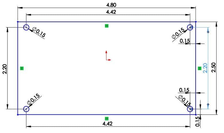
- 2.5 x 4.8 inch circuit board (allow 1 inch clearance above and below the board)

Items specifically not included with the V2 board include:
- Nominal 12 V DC external power source (0.5 A more than adequate)
- Apple remote (optional)
- Input switching hardware for multiple inputs
- Enclosure
- Display
Powered passive preamp attenuator
The V2 is powered by a nominal 12V supply (not included) which is converted to 5V for use within the board. The power drives an embedded PIC microcontroller and its interfaces with a remote control receiver, trigger outputs, USB port, 7-segment display, and most significantly the LDRs themselves which contain light emitting diodes to modulate their vaiable resistance.
The external 12V power supply also directly powers the op amps used on the V2 thus the performance of the V2 does benefit from a superior external power source.
The V2 is classified as a unity gain “passive” preamp device with no active amplification or buffering of the audio signal. That means there is no direct connection to, or manipulation of, the audio signal by a power supply. Despite the sophistication of the V25 design, each audio channel signal “sees” only a voltage divider composed of 2 LDRs in a classic series/shunt L-Pad configuration that emulates a potentiometer.
New features
The V2 introduces numerous new features many of which distinguish the Tortuga Audio LDR preamp controller from all other alternative LDR attenuators in the audio market.
Self calibration
The V2 is equipped with an integrated LDR calibration system which measures each LDR over its operating range and derives correction factors to normalize the behavior of each LDR. In the event one or more LDRs age differently and drift out of calibration, the V2 can normalize each LDR’s attenuation table to bring the unit back into precise calibration. This mitigates dependence on having to use matched sets of LDRs in each build.
Replaceable plug-in LDR modules
LDRs are similar to tubes insofar as they are nonlinear analog devices with a finite life. They have an internal LED light source, they don’t behave exactly the same from one to the next even if the same make/model, their performance characteristics can change over time, some fail early on, and they eventually age and die (although 50,000 hours is a long life). Wouldn’t it be nice to just yank a bad one out, and stick in a nice new one for around $20? Done!
Firmware updates via USB
The V2 uses an on-chip USB bootloader which allows software updates to be handled via a USB connection to a PC. Thus, software updates can downloaded from our website out and owners can upload the latest software into their V2 board from their laptop/desktop PC.
Control interfaces
The V2 has various control interface headers, solder pads and screw terminals that allow users to implement a complete preamp attenuator and controller. These are each discussed below.
Power Terminal | J6
V2.J6 is a 4 position screw terminal located in the top right corner of the board (not circled in board pic).
| Terminal ID | Description |
|---|---|
| J6.12 | +12 V DC power |
| J6.G | Power ground (connect to star ground) |
| J6.5V | External source of 5V DC power in lieu of using the built in 5V regulator. Removing the installed 5V regulator recommended. |
| J6.12T | 12V trigger out. Gets switched on/off when preamp gets turned on/off. 12V source is the same 12V source connected to J6|12. |
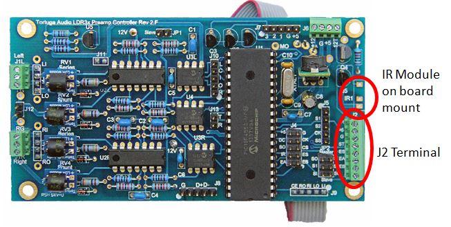
Terminal J2
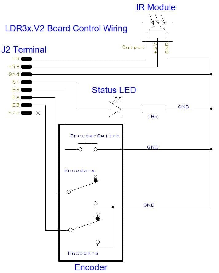
J2 is a 8 position (only 7 used) , 0.1 inch pitch screw terminal connector located on right end of the LDR3x.V2 board as shown in the image below. Below this image is a typical control wiring diagram showing the IR module, status LED and encoder connections to terminal J2. Further below the diagram is a tabular listing of the the J2 terminal connections.
| Terminal ID | Description |
|---|---|
| J2.IR | Input | Pulse signal from IR receiver module installed on board |
| J2.5V | Power | 5 volt DC power |
| J2.GND | Power | control power ground |
| J2.ST | Output | Status LED output signal. There is no current limiting resistor in this 5V output signal. |
| J2.ES | Input | encoder push button switch |
| J2.EA | Input | encoder leg A switch |
| J2.EB | Input | encoder leg B switch |
| N/C | no connection |
IR receiver | J2.IR
The IR receiver is a 3 wire module that can be mounted externally on a DM1 7-segment display module or soldered directly into the V2 board via the 3 hole board mount located just above the J2 terminal block. The IR receiver module should be oriented such that the “bump” on the receiver is facing out from the board’s edge. Due the offset spacing of the 3 IR receiver legs it’s almost impossible to not get this right.
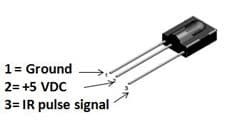
Carefully note the identity of each of the 3 IR receiver module legs. Incorrect wiring of the IR receiver can quickly destroy the receiver so be very deliberate when connecting the IR Module to the V2 board. If you locate the IR Receiver external to the LDR3x board, pin 1 must be connected to common ground (J2.Gnd), pin 2 must be connected to +5 volt power (J2.5V) and pin 3 must be connected to J2.IR. Connecting wires to an externally mounted IR Module pins is an awkward exercise in soldering. We recommend using our DM1 Display Module which provides a mounting location for the IR Receiver on its circuit board.
Regardless of where you choose to locate the IR Receiver, it must have reasonable line-of-sight access to the handheld IR remote. The most common approach is to have the IR Receiver be “looking out” from the front panel of whatever enclosure you use to house the LDR3x.
Status LED | J2.ST
J2-ST is an output signal that when connected to an LED provides status information on the V2. The positive lead of the LED (the longer lead) connects to J2-ST which provides +5 V when the LED is turned on. The negative leg of the LED (the shorter lead) connects to common ground (J2-Gnd). In most cases you’ll want to place a resistor in series with the Status LED to limit current (and brightness) through the LED. We recommend a 10-30k resistor but this will ultimately depend on the specifications of your LED and your desired brightness.
The Status LED provides the following information
- Multiple Brief Flashes: Upon unit being powered up or turned on, or anytime the Enter key is pressed.
- Steady On: Unit is on, is Un-Muted and is in normal Volume Adjust Mode (default).
- Blinking Slowly: Unit is either Muted or at maximum Volume.
- Blinking Rapidly: Unit is in Balance Adjust Mode.
- Blinking Very Rapidly: Unit is in Remote Pairing Mode.
- Brief Flash Every 2-3 Seconds: Unit is off but is running auto-calibration.
Encoder inputs | J2.ES J2.EA & J2.EB
These 3 inputs are for interfacing the LDR3x.V2 with a rotary ecoder with integral push button switch. The Encoder switch is terminated to J2.ES. J2.EA and J2.EB the “A” and “B” legs of a rotary encoder. The common leg of the rotary encoder must be connected to electrical ground (J2.Gnd).
The LDR3x was designed and tested to work with the Alps EC11 series of encoders and more specifically the model EC11B15242AF although probably any of the EC11 encoders (or equivalent) will work.
Pairing With Remote | J2.ES
There is one control function that can only be done via the Encode switch or some other switch connected via J2-ES. This control function involves pairing the V2 with the Apple Remote. Please refer to the preamp controls section on Apple Remote pairing.
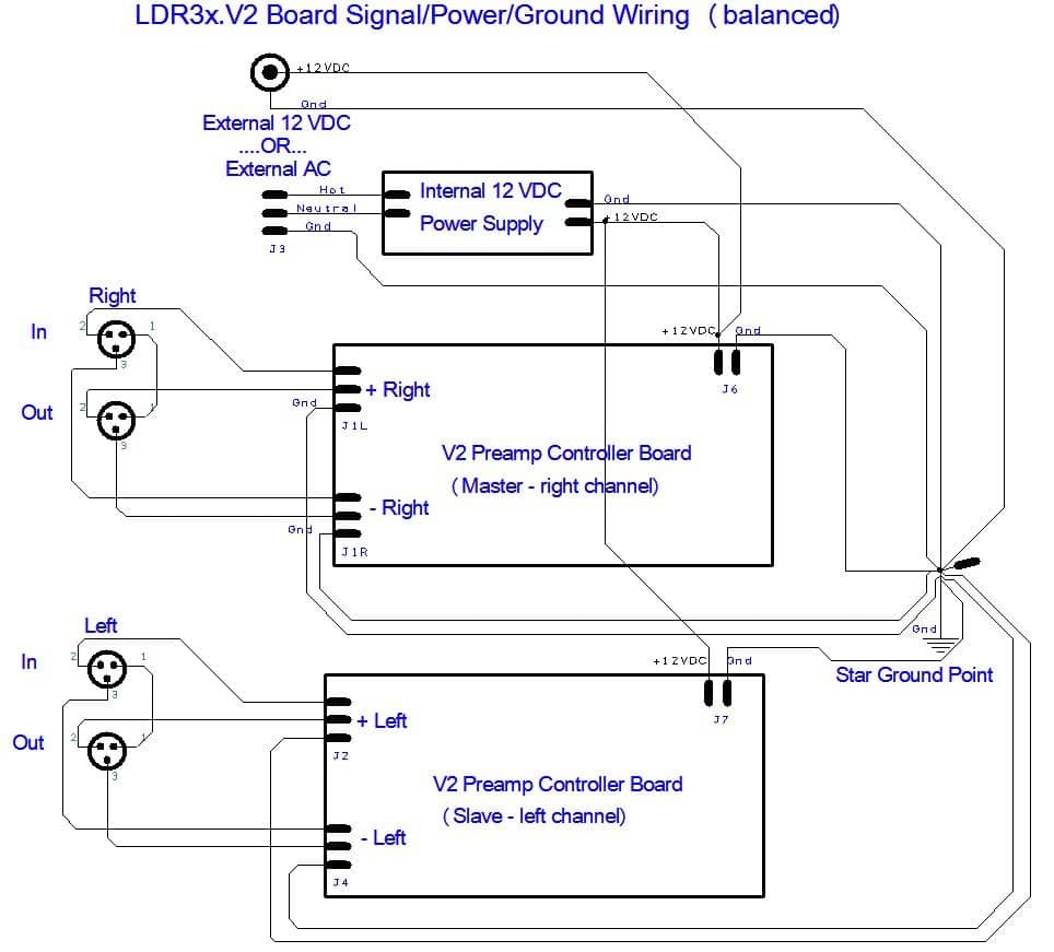
Star grounding
There’s an abundance of info available online regarding audio and grounding. Why? Because poor grounding can bugger up any audio system and it’s all too easy to get it wrong. The most reliable approach to grounding is to use “star grounding”. In simple terms, star grounding means everything that needs to be grounded gets its own dedicated connection to one single common ground point. No daisy-chaining of ground connections. This is clearly illustrated in the diagrams below. Can you spot the daisy-chained violator?
The diagrams below show both the left and right (unbalanced) and the + and – (balanced) audio signal grounds each being individually tied to star ground. These connections are absolutely essential to the proper functioning of the V2’s calibration feature. Moreover, power ground must also be connected to the same star ground point regardless of whether you’re using an external DC power supply or bringing in a 3 wire AC main to power an internal power supply unit.
Single Ended Wiring
Single ended (or “unbalanced”) audio consists of single left and right channel audio signals which are each referenced relative to ground. The left channel input and output are terminated to J1L-Input (or LI) and J1L-Output (or LO) respectively. Similarly, the right channel input and output are terminated to J1R-Input (or RI) and J1R-Output (or RO) respectively.
Input, output and ground for both the left and right channels can be terminated via the J1L and J2L screw terminals respectively. A more permanent and maintenance free alternative to using the screw terminals is to solder the audio input, output and ground via the solder pads adjacent to the screw terminals. These are marked as LI, LO, and LG for the left channel and similarly RI, RO, and RG for the right channel.

Balanced Audio Wiring
Two (2) V2 boards are required for balanced audio. The Primary handles the right stereo channel and the Secondary handles the left stereo channel. The Primary handles all communication with the user including command inputs from the remote or encoder and output to the display module etc. There is no user interface directly with the Secondary board.
Designating the secondary board (left channel)
All V2 boards operate in Primary mode unless told otherwise. To designate a V2 board as a Secondary, the pins of jumper JP1 must be connected together. A 2 pin shunt is provided for this. JP1 is circled in red in the second board above.
Primary/Secondary communication
The V2 Primary conveys necessary information to the Secondary via a 2 wire serial data link and a single wire secondary select command line between the 2 boards. These connections are shown in the red circles and arrows in the picture above. Please pay close attention to notes 1 through 4 in the picture above. Note that T-J13 on Primary connects to R-J13 on Secondary and likewise R-J13 on Primary connects to T-J13 on Secondary.

For balanced audio, you will need a pair of V2 boards. The primary board is designated for the right channel and the secondary board handles the left channel. The + channel terminates in J1L and the – channel terminates in J1R. This is arbitrary but it helps to be consistent to both avoid and help diagnose any problems. We recommend the XLR Pin 1 shields be connected together as “pass through” so that the whole “Pin 1 problem” is dealt with at your source and amp and not also at the preamp. A great article on the Pin 1 problem can be found here.
Specifications
The specifications for the LDR3x.V2 (“V2”) preamp controller board include the common specifications plus the following:
- Input/Output Type: Unbalanced stereo (single V2 board) and balanced stereo (pair of V2 boards)
- Inputs: Single input to board itself. Can switch/select up to 3 inputs when interfaced with compatible input relay/switching board.
- Outputs: Single output from board. Can be paralleled externally to accommodate additional outputs
- Input Control Interface: 0.1 inch (2.54 mm) pitch IDC pin header for connecting to optional IO3 input relay board
- Audio/Control Interface: 0.1 inch (2.54 mm) pitch mini screw terminal blocks for interfacing with Encoder, Status LED etc. (see info in other sections above for details)
- Display Module Interface: 0.1 inch (2.54 mm) pitch IDC pin header for connecting to to optional external DM1 display module (purchased separately)
- Optional Display: Drives optional single or dual DM1 numerical display(s) providing volume and status information
- Control System: 12 bit digital-to-analog circuitry used to regulate the LDRs.
- Software Update via USB : Control system software can be updated by downloading latest version from the website and then uploading it into the V2 preamp using a simple upload application (also downloaded from website) that runs on a PC connected to a USB port on the V2 board.
- USB Port: USB port for updating control system software if warranted.
- Auto Calibration: A self-contained software driven process initiated by the user that recalibrates each LDR to correct for drift/aging of the LDRs as needed.
- Replaceable LDR Modules: Similar to tubes, LDR modules can be easily unplugged and replaced in the event one fails or goes sufficiently out of calibration to warrant replacement.
- Control Methods & Functions: Remotely controlled via the elegantly simple Apple Remote and also via a rotary encoder with integral push button switch.
- Power Draw: On: < 0.4 amp @ 12 VDC | Off: < 0.25 amp @ 12 VDC
- Weight (unit): ~ 2.7 ounces
- Dimensions – As Shipped: L=8.7″ W=5.4″ H=1.75″
- Dimensions – Board : The version 2 board dimensions are almost the same as the version 1 board except that the version 2 board is 0.1 inches longer than version 1. Hole spacing is approximately the same. Hole diameter is exactly the same. The version 2 board requires an absolute minimum of 1.625 (1 & 5/8) inches of vertical space not including any standoffs used in mounting the board to a chassis. Highly recommend that 2 inches of vertical space be allocated for the version 2 board. The is twice the vertical space needed by the version 1 board and is due to an additional piggy-back board mounted on the main version 2 board.