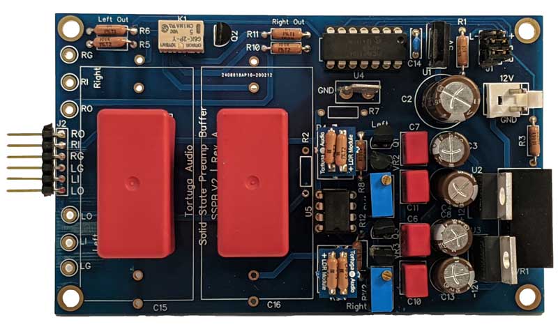
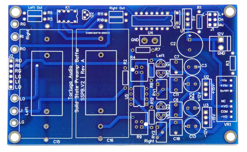
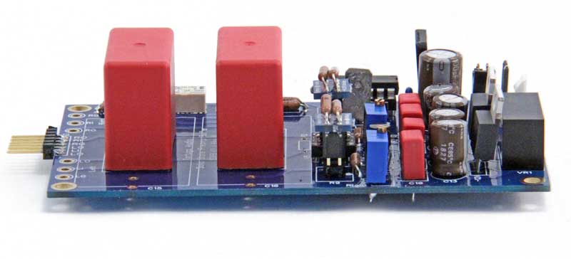
SSPB.V2 Solid State Preamp Buffer
$219.00
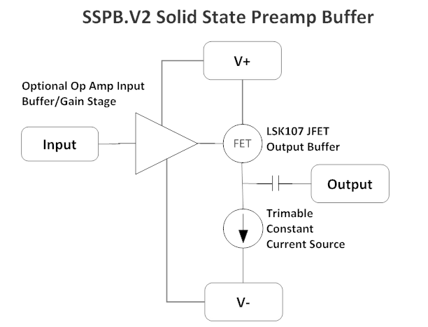
The SSPB.V2 Solid State Preamp Buffer (the “SSPB” or “buffer”) is an elegantly simple high performance solid state JFET buffer with flexible configuration options including an optional op amp input/gain stage and the ability to run the buffer as a pure direct coupled input & output discrete buffer.
The kit is geared towards the audio DIYer who is looking to add a solid state buffer to an existing passive or active preamp to improve performance due to impedance mismatch or are looking to increase system dynamics.
When equipped with a volume controller on the front end (not included in this kit) the combined volume control/buffer becomes an effective active preamp with or without gain.
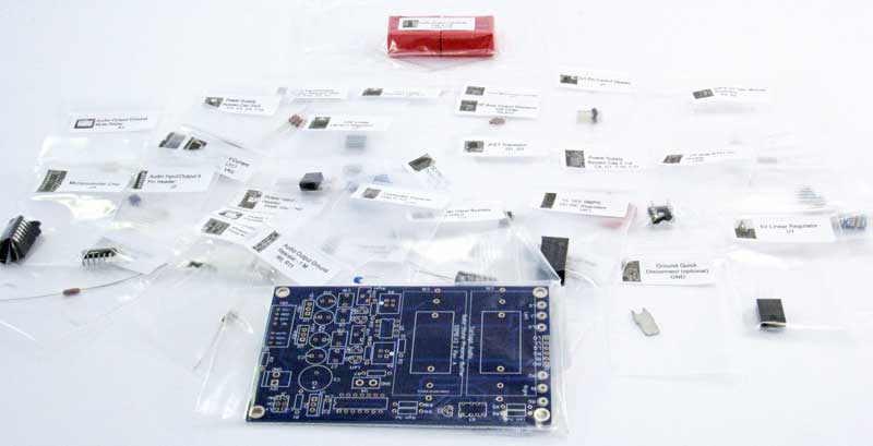
The kit is supplied as a “bag of bag of parts” and requires assembly via soldering. When fully assembled this buffer kit is a circuit board populated with parts. The kit does NOT currently include an enclosure, interface sockets, jacks, wiring or other items typically needed to build a finished stand alone buffer product. Those items are left to the DIYer to source, assemble and integrate.
Out of stock

Overview
The SSPB.V2 Solid State Preamp Buffer (the “SSPB” or “buffer”) is an elegantly simple high performance solid state buffer with flexible configuration options. In its default configuration the buffer has a direct coupled input and an AC coupled output (coupling capacitor).
The buffer can be optionally equipped with an op amp input stage. The op amp can be configured as a pure unity gain input buffer or as a gain stage with user adjustable gain.
The split voltage power supply together with the ability to hand-trim the constant current sources allows the buffer’s outputs to be optionally direct coupled with no coupling capacitor.
The buffer output stage is a discrete high performance LSK170 JFET transistor that provides robust current amplification with low output impedance and minimal DC offset.
High Quality Kit
The kit includes [24] unique premium quality parts for a total of [43] items including:
- Gold/nickel plated 2.7 x 4.4 inch printed circuit board (PCB)
- Vishay/Dale resistors in the signal path
- Vishay and Wilma polypropylene film resistors
- Elna Silmac II silk wound electrolytic capacitors
- TI LME47920 high performance audio op amp (optional)
- Most pins, jumpers and sockets are gold plated
All parts come in individual clear plastic bags with labels for easy identification.
A complete parts list will be added here soon.
Design Origins
The SSPB.V2 is a second generation version of the solid state buffer used in our LDR300.V25 Buffered Preamp which was well received by our customers. The V2 version of the buffer builds on that experience resulting in a smaller more flexible design that will enhance the performance of any passive or active preamp with clean, clear, robust current drive and optional voltage gain.
The solid state heart of this buffer is also used in our current production TPB.V1 Hybrid Tube Buffer and LDR3000.V25 Hybrid Tube Preamp.
Some have pointed out that this design appears similar to the popular Nelson Pass B1 Buffer. While not intimately familiar with the Pass buffer when we developed our own buffer deign a subsequent review does confirm both similarities and key differences. Differences include a split voltage design, direct coupled input, an adjustable constant current source, the option of running with a direct coupled output (no coupling capacitors), and the option of adding an op amp input buffer/gain-stage. After extensive evaluation of various discrete resistors we selected the excellent LSK170b JFET as the heart of the buffer circuit.
Requirements & Exclusions
The buffer kit is not an especially difficult kit to assemble but it does require the ability to solder a wide variety of through hole parts. In addition to a soldering iron you will need a decent set of wire cutters and ideally a volt-ohm meter.
None of the parts are known to be especially highly heat sensitive but common sense dictates caution when soldering smaller components especially integrated circuits.
This kit does NOT include any of the following:
- wiring to/from the buffer for power and signals
- volume control/attenuator
- amplifier
- enclosure
- power supply
- interface jacks, plugs or sockets for power and signals
Features
Kit or Assembled/Tested
The SSB.V2 is offered as a DIY kit by default. All parts come labeled in bags with every part to be inserted into the provided circuit board and soldered. All parts are through-hole. There are no surface mount parts. You can also order the board fully assembled and tested for an additional cost.
Direct Input Coupling
There is no AC input coupling capacitor. Minor DC offset on the input signal is readily accommodated (see Optional Direct Coupled Output).
Optional Gain Stage
Comes equipped with an optional dual (2 channel) op amp input stage that can be set up as a unity gain buffer or as a gain stage with fixed gain via plug-in gain modules. The buffer accommodates a wide variety of your favorite op amps. The op amp is a standard dual channel configuration 8 pin DIP that is socketed for easy removal and substitution.
Adjustable Gain
The gain of the the op amp input stage can be adjusted from unity (zero gain input buffer) to the maximum recommended by the op amp by using simple plug-in gain modules with 2 resistors each. Two gain modules are required, one for each channel.
Optional Direct Coupled Output
The buffer board comes equipped with output coupling capacitors but you can choose to run direct coupled (no AC coupling caps). Direct coupling is possible due to the split voltage power supply together with the ability to manually trim the DC offset to essentially zero. Please note that there is no excessive DC offset output protection circuitry present.
ternally the buffer employs a switching regulator that produces a +/-15V split voltage that is then further reduced to +/-12V via a second stage pair of linear regulators. If desired, you can substitute higher performance Belleson SuperRegulators for the ultimate in low noise, high performance power supply for powering the buffer and also the op amp if present.
Control Inputs | Power On & Mute
The buffer board accommodates 2 external control inputs that operate between 0 and 5 volts – PowerOn and Mute.
When PowerOn is held low, the buffer will turn on and after 3 seconds it will automatically unmute provided the Mute input is also held low. Setting PowerOn high will immediately Mute the unit and then turn off power to the op amp and buffer circuit.
Once the buffer is powered up, the buffer can be muted (+5V) and unmuted (0V) via the Mute input. Muting is done via a relay which connects the buffer’s outputs to ground while the unit is muted.
If neither the PowerOn or Mute inputs are used, both inputs must be jumpered in order for the buffer to operate when power is applied to the board.
Detailed Assembly Instructions
Assembly instructions can be found here in our online product documentation.